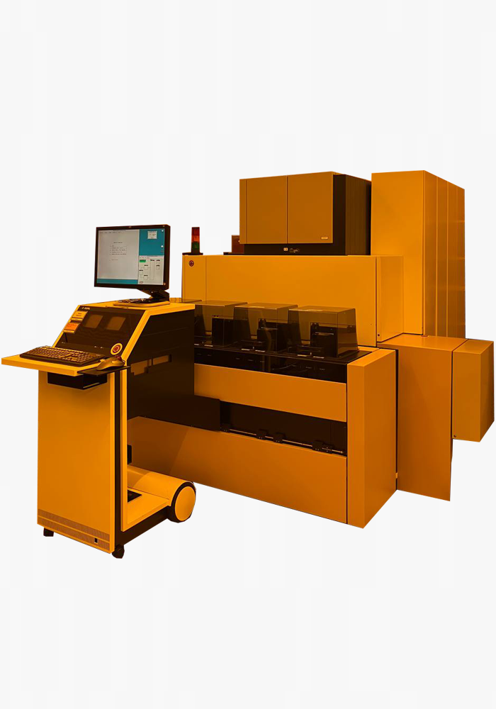
ASML Stepper PAS5500/80
The PAS 5500/80 stepper provides automatic alignment and exposure of photoresist films. It exposes one die at a time with i-line or 365nm UV light before stepping over to the next die. The image that is exposed is formed by transmitting this UV light through a patterned chrome layer on a quartz reticle or photomask. Due to the 5X image reduction of the projection optics, the exposed image on the wafer is smaller and therefore at higher resolution than the pattern on the reticle.
Optics:
Wavelength: 365 nm.
NA: 0,48.
Resolution: 0,5 µm.
Usable Depth of Focus: 1.8 µm.
Multi step imaging: focus offset up to ±200 µm.
Image scale reduction: 5X.
Alignment:
Accuracy: 8 nm.
Overlay: 45 nm.
Backside alignment is available (3DAlign).
Illumination:
Minimum exposure dose: 40 mJ/cm2.
Intensity: 400 mW/cm2.
Uniformity: <±2%.
Standard substrates: 4 inch (100 mm) wafers, technically configurable for 6 inch (150 mm) and 8 inch (200 mm) wafers. Substrate acceptable thickness range: 400 µm – 1200 µm. Wafers with through etched features or deep cavities on the backside may require to be placed on carrier wafers.
Maximum bow: ±40 µm (measure with Flexus stress meter if uncertain).
Room Temperature only.
SEMI-clean tool: for contaminated wafers (i.e. red metals), carrier wafers need to be used alongside the red wafer cassettes. Ask the tool responsibles about the different types of carrier wafers.
Reticle / photomask:
Material type: Ultra-low thermal expansion quartz.
Nominal reticle size: 6 x 6 inch (152.40 x 152.40 mm).
Default reticle thickness: 0,120 inch (3,05 mm).
Multi image reticle default configurations: 4 images (10x10 mm2), 9 images (6x6 mm2).
Field size:
Default field size (wafer level): 10x10 mm2, 15x15 mm2, 20x20 mm2.
Throughput:
Standard exposure jobs on 100 mm diameter wafers: > 95 wafers/hour.
Batch streaming: load and unload cassettes with 25 wafers at a time.
