Stirring of Light!
We propose to fundamentally study and manipulate the optical phase space density for light – as it were “stirring of light” through phase space – by combining insights gained from optical wavefront shaping with advanced structures made by colloidal self-assembly. As a result, we will be able to convert photons as efficiently as possible to other targeted forms of energy such as electric power, or transfer the energy of light to a different color. We wish to apply these concepts to realize a technology push for real devices such as solar cells, LEDs and broadband sources. Therefore we have assembled a team of fundamental and applied researchers, including experimentalists and theorists, as well as researchers with a part-time industry affiliation.

Research objective
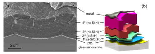
In order to pursue the direction of photovoltaic cells, we fabricate nanophotonic media from silicon with which we have experience. To this end, we use the advanced technological infrastructure available at Delft University of Technology to fabricate thin-film based structures. These structures are employed to investigate the effect of wavefront shaping on the absorption of light in a thin absorber layer. As absorber layer we use amorphous silicon (a-Si) and nanocrystalline silicon (nc-Si). The wavefront shaping is first realized by a suitable surface texturing of a film such as ZnO or TiO2 scatterers. Secondly, we manipulate the volume nanostructure of the material. The test structures consist of a thin a-Si or nc-Si absorber layer sandwiched between the scatterers.
In the first case we use surface texturing to manipulate the wavefront shaping. PVMD has built an excellent expertise in manipulating surface textures by developing a concept of modulated surface textures. This concept allows superimposition of several surface morphologies and has been tested in solar cells. On top of a film with an appropriate surface texture a thin a-Si layer is deposited. Due to the conformal growth of a-Si on the textured surface of the scatterers the surface of the thin a-Si layer is also textured. The structure is finished by depositing a thin layer of the scatterer material to obtain a structure related to the “photonic cappuccino”.
Publications
- F.T. Si et al., Quadruple-junction thin-film silicon-based solar cells with high open-circuit voltage, Appl. Phys. Lett. 105, 063902 (2014).
Stirring of Light!
Subsidy: FOM
Duration: 2012-2016
People involved: Dr. Olindo Isabella, Fai Tong Si (PhD candidate), Theodoros Papakonstantinou, Adwait Apte

