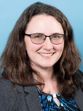

K.M. (Karen) Dowling PhD
K.M. (Karen) Dowling PhD
Profile
Awards
- 2021 – Delft Technology Fellowship, accepted 2022
- 2018 – Stanford Graduate Internship Experience in Germany Fellowship
- 2015 – 2018 National Science Foundation Graduate Research Fellow
Expertise
- Gallium Nitride, Silicon Carbide, Gallium Oxide
- Power Semiconductor Devices
- Microelectromechanical Systems
- Hall Effect Sensors
- Microfabrication
Biography
Dr. Karen Dowling was born in Seattle, USA in 1991 and grew up in Ann Arbor, Michigan. She recieved her B.S. degree in electrical engineering from the California Institute of Technology in 2013. She obtained her M.S. and PhD in EE from Stanford University in California, USA in 2015 and 2019, respectively. Her thesis focused on creating high quality magnetometers for extreme environments using Gallium Nitride, as well as some micromachining techniques in Silicon Carbide, both wide bandgap semiconductors. Before joining TU Delft, she was a postdoctoral researcher at Lawrence Livermore National Laboratory (LLNL), expanding her work to RF opto-electronic power devices known as photo-semiconductor switches. She joined TU Delft as an assistant professor in August 2022. In the Department of Microelectronics , Dr. Dowling is excited to combine both her love of sensors for harsh environments with optically coupled conduction mechanisms to open new avenues for high performing microsensors across the spectrum from fundamental research to device development and (someday) deployment.
Expertise
Publications
-
2024
3D Hall-Effect Magnetometer Using a Single Inverted Pyramid Structure
Jacopo Ruggeri / Jannik Strube / Karen M. Dowling
-
2023
Observation and Modeling of Near-Bistable Dark-Mode Current-Voltage Characteristics in Semi-Insulating Gallium Arsenide with Implications for Photoconductors
Yicong Dong / Karen Dowling / Soroush Ghandiparsi / Lars Voss / Shaloo Rakheja
-
2023
Overview of Wide/Ultra-Wide Bandgap Power Semiconductor Devices for Distributed Energy Resources
Sudip K. Mazumder / Lars F. Voss / Karen Dowling / Adam Conway / David Hall / Robert J. Kaplar / Greg Pickrell / Jack Flicker / Andrew Binder / More Authors
-
Courses 2024
Courses 2023
Media
-
2024-03-11
New Frontiers: Microelectronics Exploring Earth's Extremes and Beyond | Microelectronics at TU Delft
Appeared in: YouTube
-
2024-03-02
Up Close And Personal | Microelectronics at TU Delft
Appeared in: YouTube