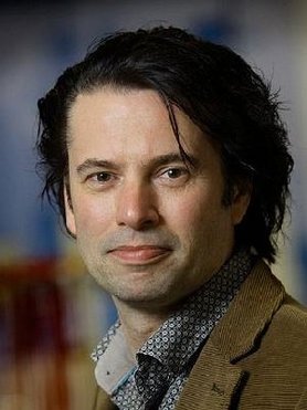

Prof.dr.ir. A.H.M. (Arno) Smets
Prof.dr.ir. A.H.M. (Arno) Smets
Professor
Arno Smets was born in 1974 in Maasbree in The Netherlands. After finishing his high school education at the Bouwens van der Boye College in Panningen in 1992, he studied physics at the Eindhoven University of Technology (TU/e). In December 1997 he finished his Masters in the Equilibrium and Transport in Plasmas group at the Physics Department under supervision of Prof. Daan Schram. At the same group he performed under supervision of Prof. Richard van de Sanden his PhD. From this point in time, his work was mainly focused on plasma processing of thin silicon films for photovoltaic applications. In the spring of 2000, Arno Smets spent 3 months during a working visit at the group of Prof. C.R. Wronski at the Penn State University and to the group of Prof. R.W. Collins at Material Research Lab in State College, USA. Arno Smets defended on May 20th 2002 his PhD thesis: “Growth Related Material Properties of Hydrogenated Amorphous Silicon”. After his PhD, he worked as a Post-doc within the Helianthos Project, which is a collaboration between Akzo Nobel (currently NUON Helianthos), Eindhoven University of Technology, Delft University of Technology, Utrecht University and TNO. In March 2005 Arno moved to Tsukuba in Japan and joined as a visiting Researcher the Research Center for Photovoltaics under leadership of Michio Kondo at the National Institute of Advanced Industrial Science and Technology (AIST). From January 2008-february 2010 he managed a collaboration between AIST in Japan, and the TU/e and NUON Helianthos in the Netherlands. From March 2010 Arno Smets is associate professor at the Delft University of Technology in the Netherlands in the Photovoltaic Material and Devices group of Prof. Miro Zeman at the faculty Electronic Engineering, Mathematics and Computer Sciences.
Arno Smets has worked on a wide variety of topics related to the plasma processing of thin silicon films for photovoltaic applications, mainly focused on the second generation technology. Among many of his research topics and achievements are: plasma technology development, development of high deposition rates of hydrogenated amorphous and microcrystalline silicon, large area deposition, development of novel in-situ diagnostics to monitor plasma processes, plasma-surface interaction and thin film growth, study of dust generation in plasma environments, study of the mechanisms involved in thin silicon growth with respect to deposition rate, temperature and ion induced film-modifications, fundamental understanding of microstructures and related properties of thin silicon films, study of instable thin silicon properties related to the Staebler-Wronski effect or oxidation of thin silicon films, processing of thin film silicon based photovoltaic devices and development of novel concepts to further enhance the efficiencies of thin film silicon photovoltaic devices.
Expertise
Publications
-
2024
Comprehensive Glare Hazard Analysis of Ethylene Tetrafluoroethylene (ETFE) Based Frontsheet for Flexible Photovoltaic Applications
K. P. Sreejith / Vijay Venkatesh / Govind Padmakumar / Arno H.M. Smets
-
2023
Strategies for realizing high-efficiency silicon heterojunction solar cells
Yifeng Zhao / Paul Procel / Can Han / Liqi Cao / Guangtao Yang / Engin Özkol / Alba Alcañiz / Katarina Kovačević / Gianluca Limodio / Rudi Santbergen / Arno Smets / Arthur Weeber / Miro Zeman / Luana Mazzarella / Olindo Isabella
-
2023
The Role of Education and Science-Driven Tools in Scaling Up Photovoltaic Deployment
Ana M. Martínez / Christian Thiel / Sandor Szabo / Imen Gherboudj / René van Swaaij / Andreea Tanasa / Arnulf Jäger-Waldau / Nigel Taylor / Arno Smets
-
2023
The native and metastable defects and their joint density of states in hydrogenated amorphous silicon obtained from the improved dual beam photoconductivity method
Mehmet Güneş / Jimmy Melskens / Arno H.M. Smets
-
2022
Application of metal, metal-oxide, and silicon-oxide based intermediate reflective layers for current matching in autonomous high-voltage multijunction photovoltaic devices
Thierry de Vrijer / Sander Miedema / Thijs Blackstone / David van Nijen / Can Han / Arno H.M. Smets
-
Media
-
2022-11-15
Energie in 2030: wat gaan de bronnen ons brengen?: 5 specialisten belichten 5 duurzame energiebronnen
Appeared in: E&W Installatietechniek
Ancillary activities
-
2022-12-01 - 2025-02-01
Electricity, natural gas, steam and air conditioning supply