Huge machine seduces stubborn atoms to crystallise
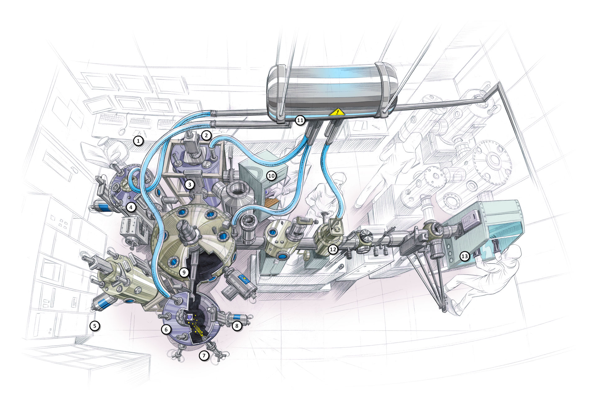
It takes impressive and expensive machinery to control processes at the nanoscale. For the fabrication of semiconductor nanowires at Microsoft Quantum Lab Delft, Microsoft invested millions in the MBE (Molecular Beam Epitaxy) machine. It is located in one of the clean rooms of the Van Leeuwenhoek Laboratory.
Senior researcher Dr Philippe Caroff takes the science editor and the illustrator for a first tour to see the MBE machine. No paper is allowed inside and visitors need to put on dust-free overcoats, boots and gloves. The multimillion-euro MBE machine, located in a separate room in the lab, is being used to manufacture nanowires of about 300 atoms wide (100 nanometres) and a few micrometres long. Nanowires made from semiconductor materials such as indium-arsenide or indium-antimonide, in contact with a superconductor, have been shown to be suitable host materials for Majorana particles. Majorana quasiparticles, discovered by Professor Leo Kouwenhoven in 2012, are regarded as promising candidates for quantum bits or qubits – the elementary units for the future quantum computer.
When the first Majoranas were demonstrated (Science, 12 April 2012), it was in a semiconducting nanowire made of indium-antimonide between a gold contact and a stretch of superconducting material. At the time, nanowires were grown by controlled crystallisation underneath a submicron-sized gold droplet. Caroff, senior scientist at Microsoft, calls this ‘the classic method’.
The MBE machine aims to standardise the manufacture of nanowires and to enable the production of grid-like structures instead of simple wires. The required patterns are transferred onto a piece of silicon substrate by means of electron beam lithography, a technology from the micro-electronics industry. The electron beam creates a path in the chemical resist, which is then removed to expose an insulator masking layer. Further etching removes insulator layers opening a window to the crystal below. Below lies monocrystalline semiconductor of the target, as a virgin soil for the semiconductor crystals that will guide growth in the etched submicron grooves.
But for that growth to happen, extreme requirements need to be fulfilled. The vacuum within the entire machine for instance is attainable to the highest degree. In the machine, it is just as empty as it is in space between the planets, illustrates Caroff. Grease or rubber are absolute no-gos in this installation. Inside, the mean free path before a free flying atom hits one of its neighbours is 50kilometres.
Another challenge is maintaining the heat imbalance between the high temperatures required to produce atomic vapours, and the cryogenic environment of the target for the atomic beams. Masses of liquid nitrogen, about 1,000 litres per day, circulate in double-wall cryo-panel inside the MBE to keep the MBE at the right temperatures and contribute to the ultra-high vacuum. Also, there is the atomic incompatibility. “We’re putting materials together that don’t like each other in nature,” says Caroff. Therefore, semiconductors and superconductors are applied in different deposition chambers, and a robot system transports the target in between the various production stages.
Researchers are now trying to get atoms to crystallise in the shape and composition they require. But getting an atom to crystallise is like getting a dog to lie down. You cannot force the process, you can only try to tempt it to settle. “We are discovering the psychology of atoms,” says Caroff. “We are starting to understand their stubbornness.”
