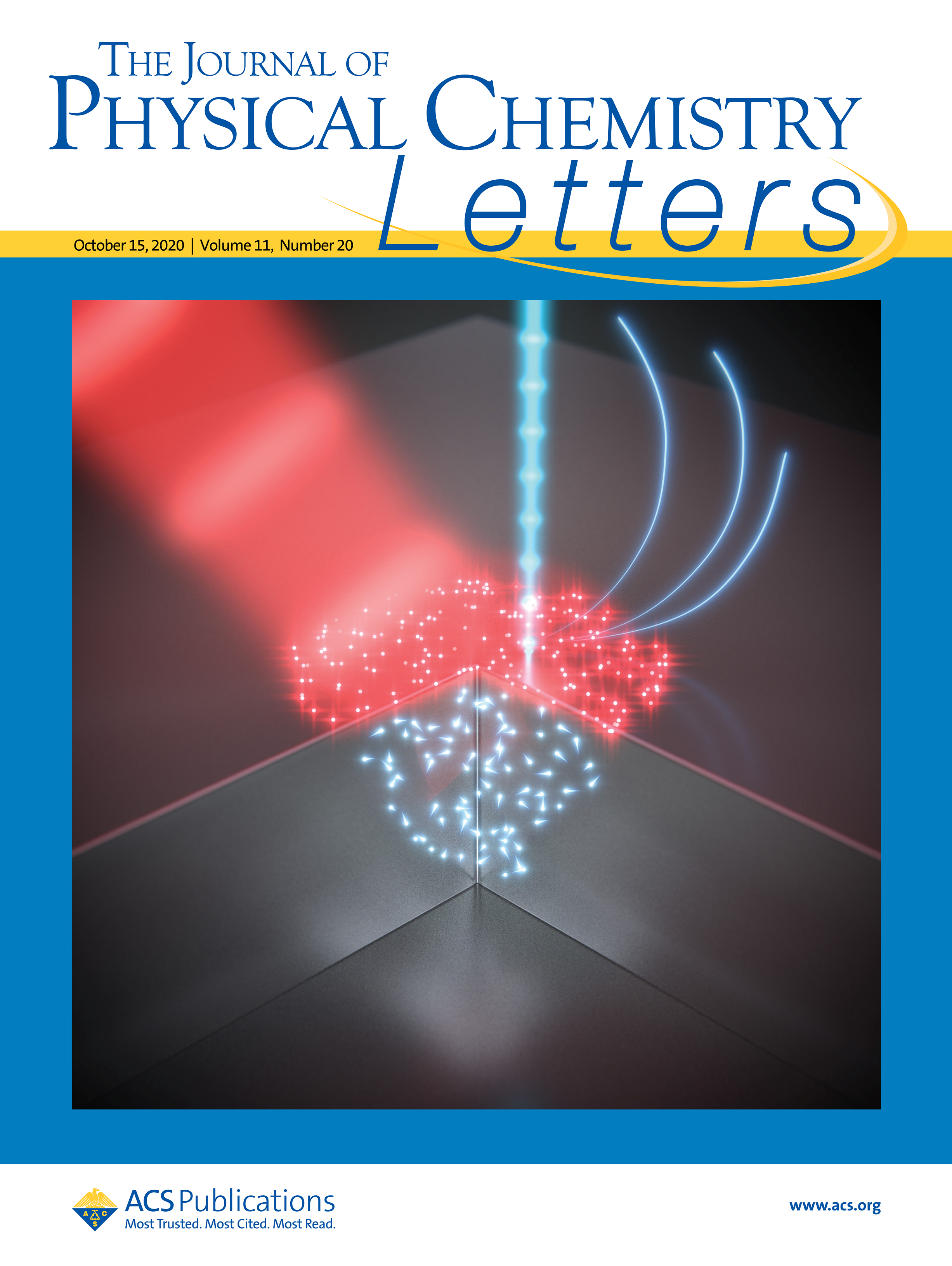
Cover article on new technique for ultrafast electron microscopy
Mathijs Garming, Pieter Kruit, and Jacob Hoogenboom (imaging physics) have published a paper in collaboration with Maarten Bolhuis and Sonia Conesa-Boj (quantum nanoscience) on a new technique for doing ultrafast scanning electron microscopy (USEM).
Newly developed lock-in USEM was used to image charge carrier dynamics on the material Gallium Arsenide. The technique allows for bulk carrier and surface trapping dynamics to be separated and individually studied. Marked differences in surface potential were found with different surface termination of the material, while only the top atomic layer was different!
These results can help gain further insight in carrier dynamics and trapping, and be beneficial to the development of cutting edge new solar cells and photodetectors.
The work has been published open access in the Journal of Physical Chemistry Letters.
Abstract:
“Visualizing charge carrier flow over interfaces or near surfaces meets great challenges concerning resolution and vastly different time scales of bulk and surface dynamics. Ultrafast or four-dimensional scanning electron microscopy (USEM) using a laser pump electron probe scheme circumvents the optical diffraction limit, but disentangling surface-mediated trapping and ultrafast carrier dynamics in a single measurement scheme has not yet been demonstrated. Here, we present lock-in USEM, which simultaneously visualizes fast bulk recombination and slow trapping. As a proof of concept, we show that the surface termination on GaAs, i.e., Ga or As, profoundly influences ultrafast movies. We demonstrate the differences can be attributed to trapping-induced surface voltages of approximately 100–200 mV, which is further supported by secondary electron particle tracing calculations. The simultaneous visualization of both competing processes opens new perspectives for studying carrier transport in layered, nanostructured, and two-dimensional semiconductors, where carrier trapping constitutes a major bottleneck for device efficiency.”
Read the article here:
M.W.H. Garming et al., Lock-in Ultrafast Electron Microscopy Simultaneously Visualizes Carrier Recombination and Interface-Mediated Trapping. The Journal of Physical Chemistry Letters 2020, 11, 8880-8886. DOI: 10.1021/acs.jpclett.0c02345.
